

“Exactly what NVIDIA's Jensen Huang is looking for right now.”
That was TechRadar's assessment after imec unveiled its latest advances in RF silicon interposer technology. A striking endorsement – and one that points to a much broader challenge facing hyperscalers and the wider AI ecosystem: how to move ever-growing volumes of data at ever-higher speeds while staying within realistic power, cost, and deployment constraints.
"In data centers especially, the pressure that surging data traffic and AI workloads place on infrastructure is mounting rapidly,” says Joris Van Driessche, portfolio director advanced RF technologies at imec. “And nowhere is that pressure more apparent than in interconnect technology.
Electrical interconnects have long been the backbone of data movement between switches, routers, and servers. Yet at longer distances and higher lane rates, their power consumption rises sharply, thermal constraints intensify, and signal integrity degrades.”
That is why the industry is accelerating its shift toward optical interconnects. Using light rather than electrical signals, optical interconnects enable data to travel faster, farther, and more efficiently. But they too are being pushed to new extremes, as AI infrastructure evolves toward (multi-)terabit-per-second interfaces that must combine ultra-high energy efficiency with extremely low (sub-microsecond) latency.
These are the requirements facing hyperscalers and the wider AI ecosystem. Meeting them demands components capable of operating at frequencies extending well beyond 100 GHz.
Combining technologies to preserve performance
The move to higher frequencies creates a fundamental dilemma. Conventional Si-CMOS technology offers the cost advantages of high-volume manufacturing, but its performance falls short at frequencies beyond 100 GHz. By contrast, III-V materials such as indium phosphide (InP) and gallium nitride (GaN) deliver superior gain, output power, and efficiency – yet remain significantly more difficult and costly to manufacture at scale.
“Early design assessments suggest that imec's RF silicon interposer technology could reduce III-V chiplet area by more than a factor of three without sacrificing functionality.”
Joris Van Driessche: “And for optical interconnect building blocks such as drivers and transimpedance amplifiers (TIAs), there’s even a third contender: BiCMOS technology – a semiconductor platform that combines the scalability of CMOS with the speed of bipolar transistors. BiCMOS can deliver the required bandwidth and performance without relying on III-V materials, but it still comes with the challenge of how to preserve that performance across the interconnects linking these drivers and TIAs to the system’s digital signal processors and photonic integrated circuits.”
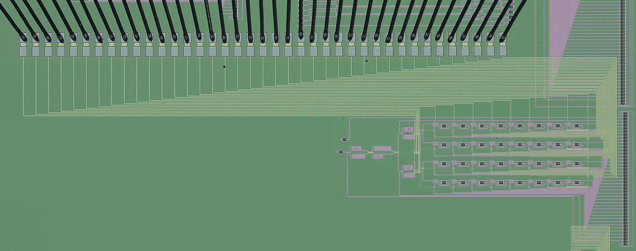
The solution, he explains, is to combine strengths. “Rather than building an entire system in III-V or BiCMOS technology, you use compact III-V or BiCMOS chiplets only for the performance-critical functions where their advantages justify the additional cost. These chiplets are then heterogeneously integrated on an RF silicon interposer that hosts the remaining passives and can provide ultra-low-loss interconnects at frequencies up to 325 GHz.”
Quantifying the benefits: a smaller footprint without sacrificing functionality
“It’s an approach that strongly resonates with hyperscalers and the broader ecosystem,” says Van Driessche. “They recognize that III-Vs and BiCMOS deliver outstanding RF performance. So, the next question is whether the economics work. RF silicon interposer technology may not be the lowest-cost option at a component level, but as systems become more complex, it has the potential to significantly reduce overall cost, footprint, and integration complexity.”
Early design assessments support that potential, suggesting that imec's RF silicon interposer technology could reduce III-V chiplet area by more than a factor of three without sacrificing functionality – while creating opportunities for enhanced RF performance. This is achieved through finer-pitch (flip-chip) integration, and by offloading passive components onto the interposer.
Ongoing work with industry partners aims to validate these projections and quantify the resulting system-level benefits through future proof-of-concept demonstrations.
Beyond data center applications
Although data center infrastructure is one of the most compelling applications for RF silicon interposer technology, its potential extends well beyond this domain.
High-performance radar systems for aerospace, security, and automotive applications face many of the same challenges. As radar moves to higher frequencies to achieve finer sensing resolution, and needs to maintain long-range detection capabilities, it requires transmitter technologies that deliver high output power and efficiency, alongside receivers with an exceptionally low noise figure.
And next-generation satellite communication systems have similar requirements too – as they migrate to higher frequency bands (Ka-, Q/V-band, and beyond) to support ever-increasing data rates.
In each of these cases, III-V semiconductor materials provide the RF performance needed to operate under demanding conditions, while RF silicon interposer technology enables their heterogeneous integration into compact, scalable, and manufacturable systems – supporting a clear path toward high-volume deployment.
The road to manufacturable high-frequency systems
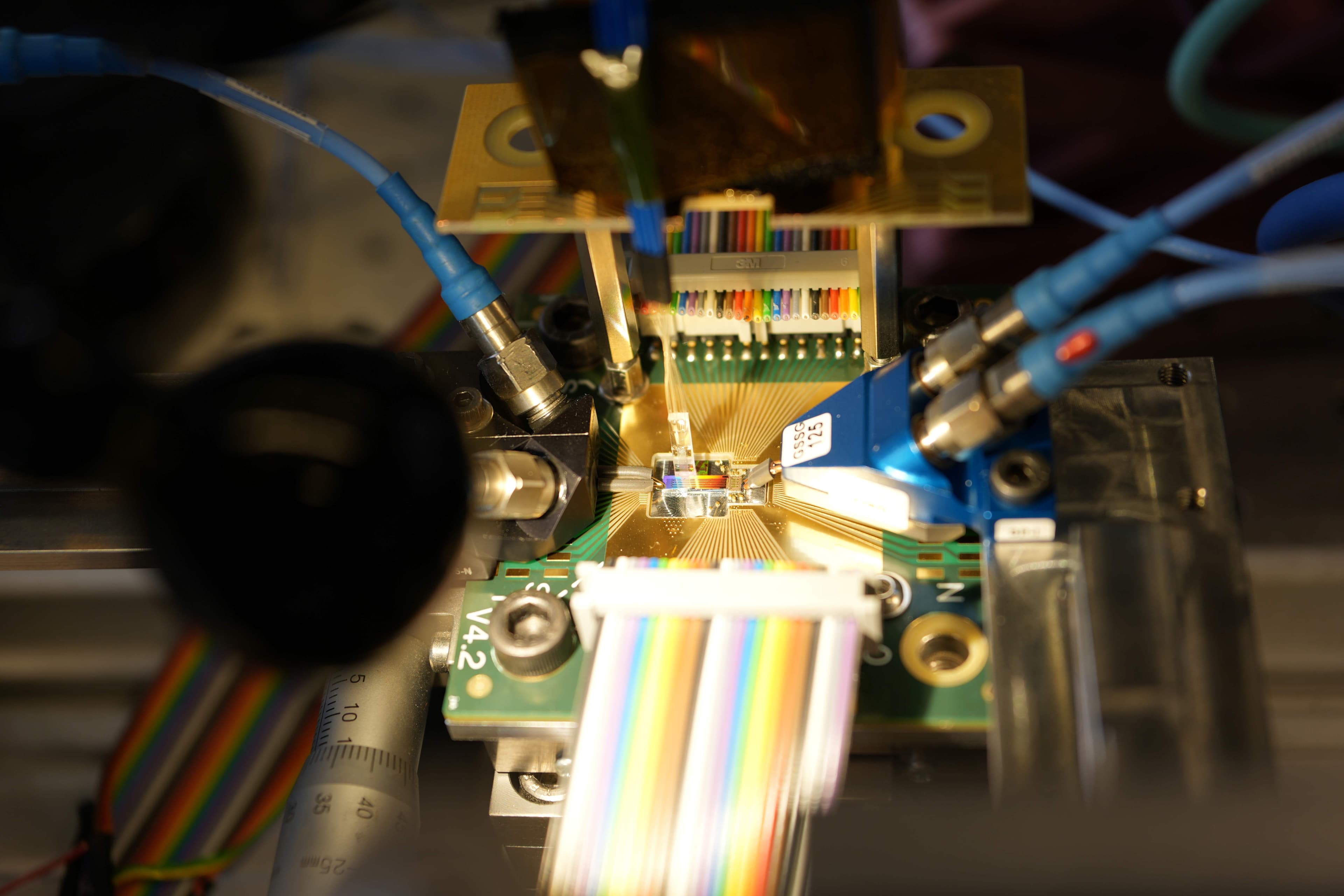
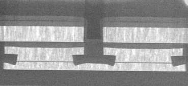
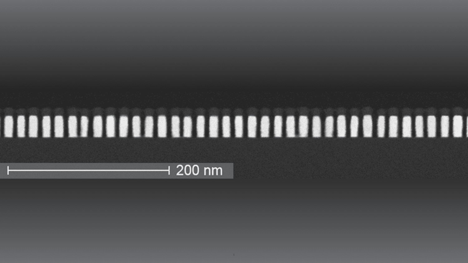
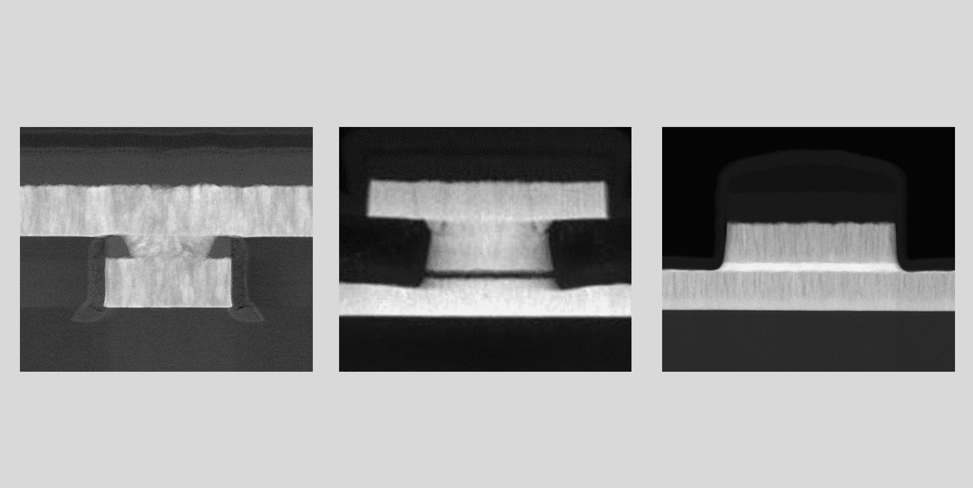
Imec has progressively evolved its 300mm RF silicon interposer technology into a system-level platform for the heterogeneous integration of III-V chiplets on Si-CMOS – its latest advances including high-density embedded capacitors, a scalable modelling framework for passive components, and laser-assisted bonding for III-V chiplet assembly.
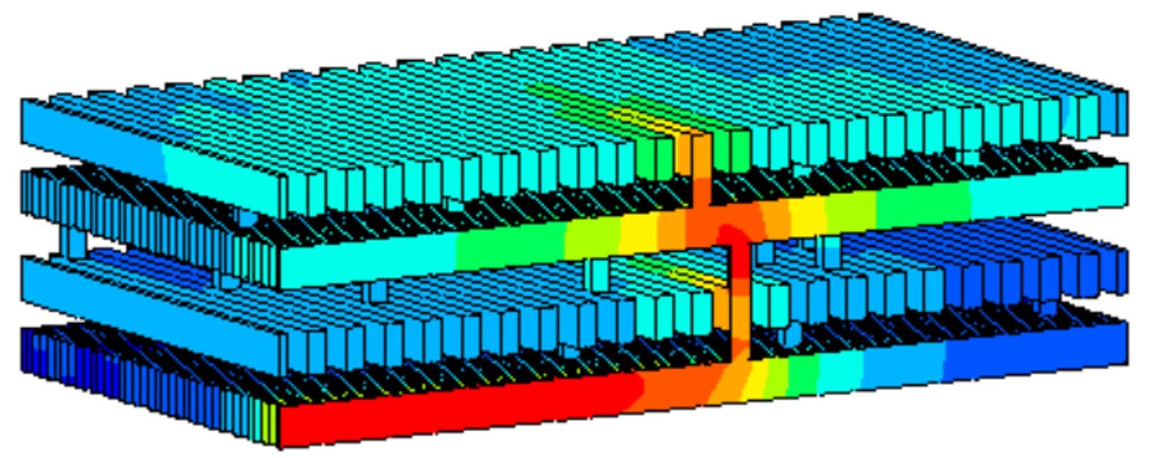
Joris Van Driessche: “The current focus is on increasing the platform's technology readiness and establishing the design flows, passive-component models, thermal-management solutions, and reliability data needed to support low-volume manufacturing.”
“A key differentiator is imec's IC-Link capability, which provides a pathway from prototyping to low-volume manufacturing. As industry attention shifts from isolated proofs-of-concept to deployable solutions, such manufacturing support will play an increasingly important role in accelerating the commercialization of next-generation extreme-bandwidth systems,” he concludes.

Joris Van Driessche received the M.Sc. degree in Electrical Engineering from Ghent University (Belgium) in 2001. He joined imec in 2001 as an RF front-end architecture research engineer, focusing on system specification and architecture definition for multi-standard RF transceivers.
In 2006, he became project manager for reconfigurable RF transceivers, addressing challenges towards true software-defined radio transceivers optimized for advanced CMOS technologies. He subsequently took on the role of program manager for imec's Advanced RF research program, focusing on millimeter-wave and sub-THz RFICs, antennas, packaging, and system design.
Today, Joris serves as portfolio director, Advanced RF technologies at imec.
Published on:
6 August 2026