
CFET technology moving forward, backed by integration efforts and DTCO studies
The semiconductor industry is going through a major architectural transition, with gate-all-around (GAA) nanosheet transistors replacing FinFETs in advanced logic nodes of 3nm and beyond. GAA nanosheet transistor technology offers scalability down to the A10 logic generation, where it enables 5.5-track (T) standard cells – the track being a measure for the standard cell height.
For the A7 node, options are becoming increasingly diverse to meet the growing diversification of application needs, driven by the AI revolution. According to imec’s latest roadmap, one option is to design systems around imec’s CMOS 2.0 scaling paradigm. With CMOS 2.0, a system-on-chip (SoC) is partitioned into heterogeneous, functional tiers each optimized using the most suitable technology, and reconnected using 3D interconnect technologies.
For other use cases, GAA nanosheet technology may be pushed to its ultimate scaling limits, with power delivered from either the frontside or the backside. But industry may as well transition to complementary FET (CFET) device architectures. By stacking p and nMOS transistors on top of each other, standard cells can be further scaled down to 3T, thereby extending the classical CMOS logic roadmap to at least the A3 technology node.
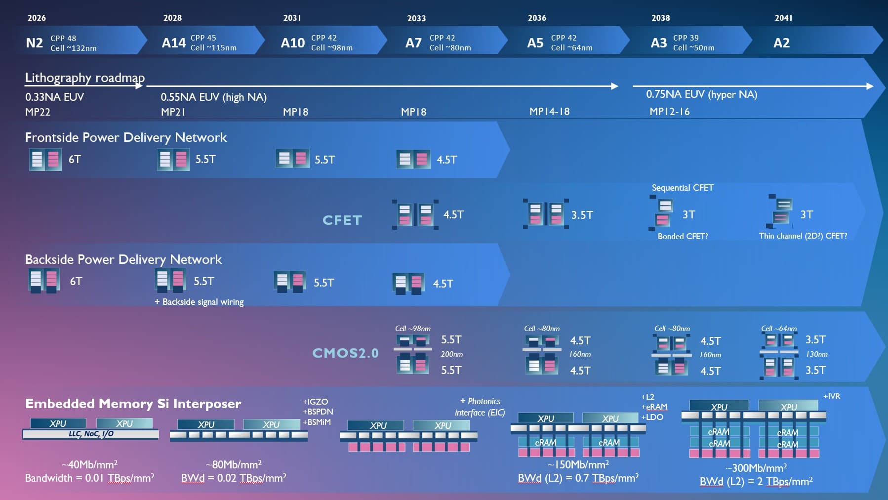
Figure 1 – Imec’s logic technology roadmap.
Do you want regular updates on imec’s semiconductor research?
Imec and its industrial partners are working to make CFET-based devices manufacturable. In recent years, they laid the groundwork for key integration approaches, categorized as monolithic CFET (mCFET) and sequential CFET (sCFET) [1,2].
Both approaches start from the vertical stacking of Si/SiGe layers from which the n and pFETs are fabricated. With mCFET, the vertical device structure with common top and bottom gates is patterned and processed in a single sequence of process steps. The patterning, deposition and selective removal of materials around and in between the high-aspect ratio device structure requires considerable effort in terms of module development. SCFET, on the contrary, patterns the top and bottom devices independently using dedicated masks. With sCFET, the individual process steps are simpler compared to mCFET but some critical steps need to be executed twice – for top and bottom separately. sCFET additionally involves two wafer flips, distorting the wafer and challenging the precise alignment of front-to-back device connections. Pending further progress in alignment accuracy, mCFET is believed to offer the fastest path to industrial adoption.
Progress in CFET integration is complemented with design-technology co-optimization (DTCO) studies that examine CFET device architectures from a circuit level perspective [2]. These studies aim to identify scalable standard cell configurations and performance boosters that offer the best tradeoff in terms of power, performance, area and cost.
In this 2-part article, we report major progress in CFET device integration, and we discuss CFET scalability using DTCO studies.
In part 1, two process modules are presented that are essential for both mCFET and sCFET device flavors: (1) a backside contact module, and (2) a gate stack integration approach that enables multiple threshold voltages (Vt) in nanosheet and CFET devices.
In part 2, a scalable architecture for sCFET will be introduced allowing both split-gate and common-gate configurations. Besides progressing the logic roadmap, DTCO work shows how this split-gate architecture also benefits CFET-based SRAM scaling. Finally, improved back-end-of-line (BEOL) routability is demonstrated, supporting the scaling of CFET standard cells.
The reported results are achieved in the framework of the imec-hosted European NanoIC pilot line, which is targeting the development of beyond-2nm systems-on-chip. CFET development, which is centered on CFET-specific designs, process steps, modules and baseline flows, has been selected as one of the key enabling technologies for extending the logic roadmap into the ångström era. This will help Europe to remain at the forefront of next-generation semiconductor innovation and manufacturing.
An improved module for backside contacting: enhanced performance and survival rate of the bottom pFETs
Throughout the development of CFET-specific integration modules, it became clear that contacting the source/drain junctions of the bottom devices directly from the wafer backside offers clear advantages over frontside contacting. Backside contacting not only improves the contact resistance of the bottom devices but also enlarges the process window for top device source/drain formation – as demonstrated by imec at 2024 VLSI [3]. It additionally provides a lever for further reducing standard cell height and for decreasing routing congestion in the BEOL at the wafer frontside.
Backside contacting in general requires additional process steps, including wafer bonding and substrate thinning from the backside. Also, an extra module is needed to electrically isolate the source/drain epi from the underlying substrate – referred to as the backside dielectric isolation (BDI) module.
The conventional BDI module: variability in the bottom source/drain structure, and large access resistance
A common approach to backside contacting integrates a BDI module that is formed entirely from the wafer backside, near the end of the process flow. But such a process flow comes with a few limitations. First, it leads to considerable variability in the volume of the bottom SiGe:B source/drain structure, as this is now seeded by both the bottom Si channel and the underlying Si substrate during bottom SiGe:B source/drain epi growth. Second, for the same reason, the SiGe:B structure consumes a lot of space that cannot be utilized by the contact metal – contributing to the access resistance into the device. And third, the process scheme induces several yield loss factors for the backside contacts - which works against industrial adoption.
A novel BDI module: improved performance and survival rate of bottom devices
At 2026 VLSI, imec demonstrated an improved backside contacting module for CFET devices [4]. The new scheme results in a fivefold improved drive current (Is) of bottom pFET devices compared to results achieved with the conventional integration scheme. The enhanced performance can be attributed to an improved access resistance for the bottom pFETs, which was reduced from 1753Ωµm to 378Ωµm. In addition, the survival yield of the bottom pFETs increased from 45% to 85% compared to previous reported results.
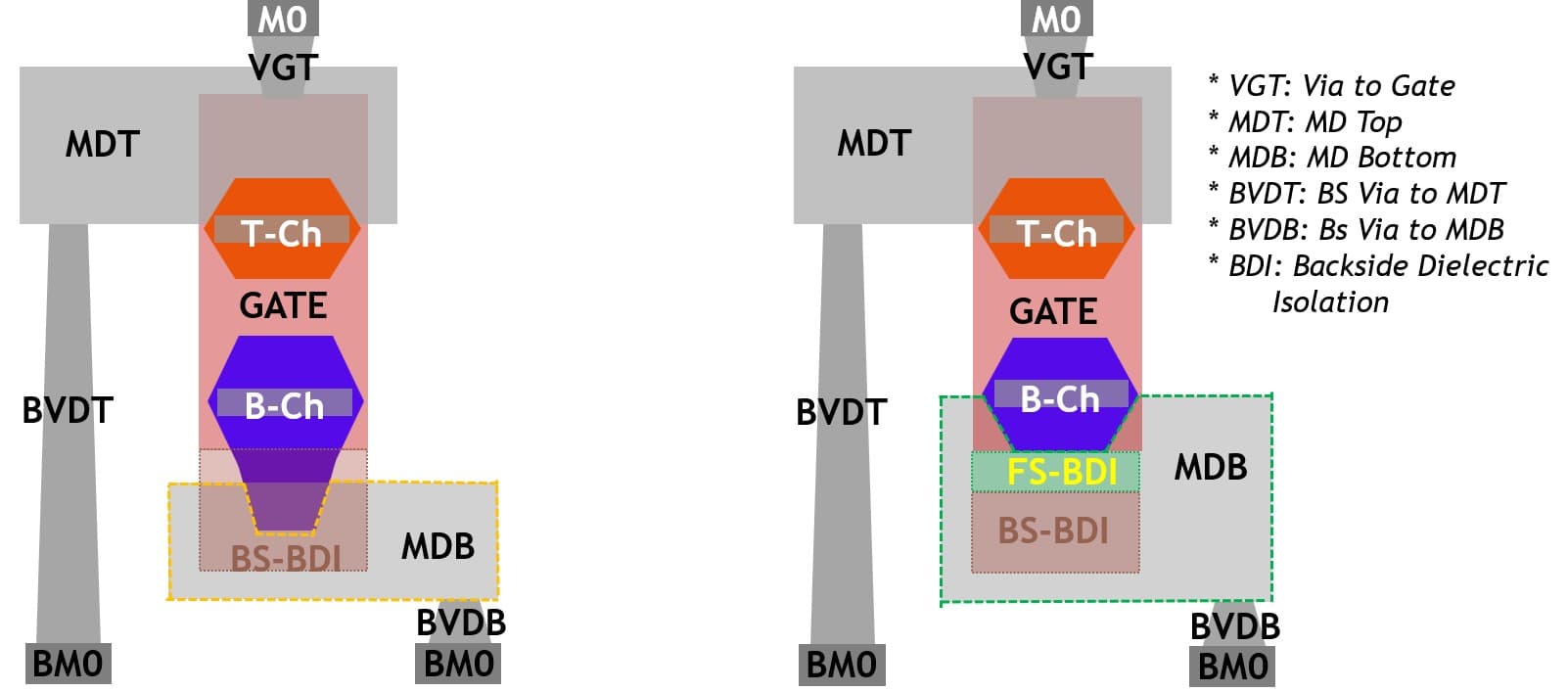
Figure 2 – Approaches to backside contacting: (a) conventional approach with a backside-formed BDI structure; (b) imec’s novel scheme with frontside BDI and backside BDI (as presented at 2026 VLSI).
A key element of the new module is the formation of an extra frontside-formed BDI (FS-BDI) structure under the source/drain, completely isolating the source/drain epi structure from the underlying substrate. As such, the bottom SiGe:B source/drain epi is no longer seeded by the underlying Si substrate during epi growth. And this improves both the variability in SiGe:B volume and the contact resistance of the device. The frontside BDI is formed early in the process flow by adding an extra Ge-rich SiGe layer to the Si/SiGe stack, which is replaced with a dielectric during middle-dielectric isolation formation (the MDI module, [1]). The frontside BDI formation step hence does not add much to the process complexity. An additional backside-formed BDI structure is added downstream in the process flow. An overall backside process optimization – involving wafer bonding, extreme wafer thinning, and backside contact etch – also contributes to the superior pFET performance.
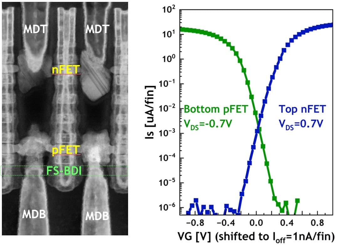
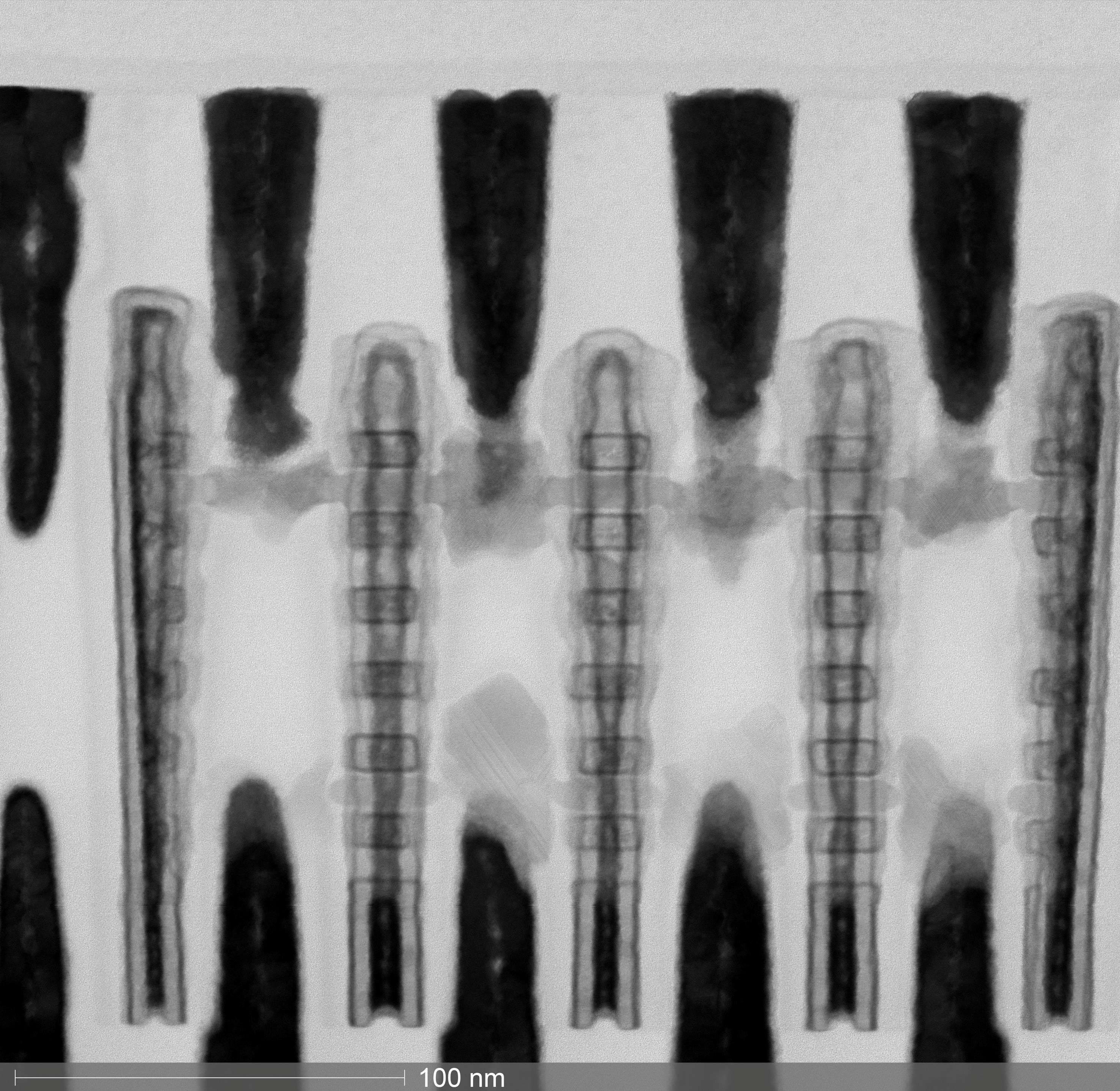
Figure 3 – (Left) TEM cross-section of a mCFET with frontside BDI and backside BDI; (b) bottom pFET and top nFET current-voltage (Is-Vg) characteristics (as presented at 2026 VLSI).
While the improved backside contact module was demonstrated on an mCFET test vehicle, the process flow is believed to be generic – applicable to sCFET devices as well.
A novel dipole-based gate stack for threshold voltage tuning: robust and thermally compatible with CFET
Stacked nanosheets form the core of both GAA nanosheet and CFET device architectures, where they serve as the channels of the active devices. But the threshold voltage (or Vt, the gate voltage at which the device begins to switch on) does not necessarily need to be the same for the various GAA nanosheet or CFET devices even within the same integrated circuit. Ideally, devices operate at a different threshold voltage to perfectly balance the competing demands of, for example, high-performance computing and ultra-low power operation.
The most obvious approach for achieving this Vt tuning is to alter the composition and thickness of the gate metals, hence changing the effective work function of the gate. But in advanced nanosheet-based devices, the space in between the stacked nanosheets is extremely tight, leaving little room for gate metal thickness variation. And this urges industry to use other approaches that do not consume extra volume.
Dipole-based multi-Vt tuning: an attractive approach for nanosheet-based devices
Dipole-based multi-Vt tuning has proven to be a promising volume-less alternative. With dipole integration, dipole-forming metal such as lanthanum (La) atoms is added between the SiO2 interlayer and the HfO2 high-k dielectric layer of the gate stack. The shifter material forms dipoles at the SiO2/HfO2 interface which affects the Vt of the device. Varying Vt values can be obtained by incorporating different concentrations of La.
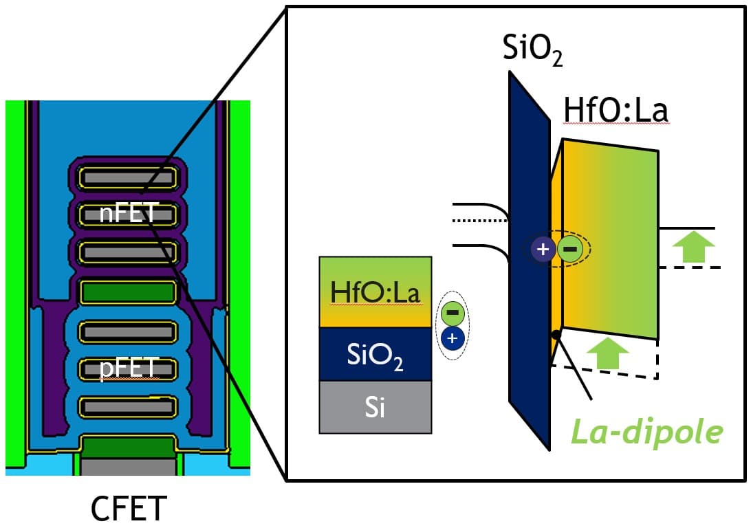
Figure 4 – General principle of the dipole-driven multi-Vt approach for nanosheet and CFET devices (as presented at 2026 VLSI).
Dipole-last vs. dipole-first integration approaches: high thermal budget vs. patterning damage
The most widely used integration approach for inserting shifter materials is the dipole-last approach, where La-oxide is deposited on top of the HfO2 high-k dielectric layer. During a high-temperature annealing step, the shifter material diffuses through the relatively thick high-k layer towards the HfO2/SiO2 interface to form a dipole. While this approach works well for CMOS devices of previous generations, the high thermal budget presents challenges for CFET-based devices that implement a low-temperature replacement metal-gate process.
Several years ago, imec’s focus therefore shifted towards a dipole-first approach, depositing the shifter material directly onto the SiO2 layer and as such avoiding the high-temperature anneal step [5]. Unfortunately, patterning the La-oxide shifter layer was observed to induce damage to the underlying SiO2 interlayer, affecting the performance of the device.
Imec’s novel dipole-middle approach: robust and compatible with CFET processing
At 2026 VLSI, imec demonstrated a novel gate stack integration scheme, referred to as dipole middle, combining the best of both worlds [6]. In this case, the shifter is deposited on a first, thin layer of HfO2. The shifter is then ‘locked in’ during a mild annealing step, sufficient for diffusion through the thin high-k dielectric layer. This thin layer of HfO2 also protects the underlying SiO2 interlayer during shifter patterning. After removal of the unreacted shifters, a second layer of HfO2 is deposited, followed by another annealing step. Using this approach, the total thermal budget can be kept lower than in the case of the dipole-last approach, especially when multiple shifter materials need to be integrated. This makes the new gate stack integration approach compatible with mCFET devices.
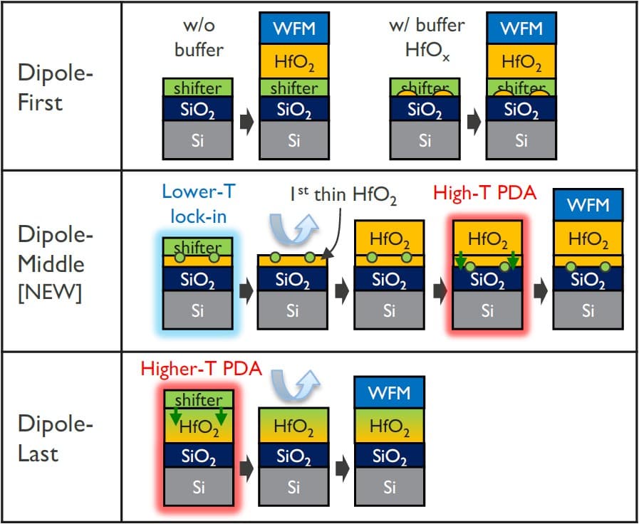
Figure 5 – Schematic representations of dipole-first, dipole-middle and dipole-last integration approaches (as presented at 2026 VLSI).
The dipole-middle approach was successfully demonstrated on a CFET-based test vehicle where only nFET top devices were made electrically accessible for evaluation. The electrical data showed a small, but consistent nFET Vt reduction of about 30mV compared to a reference where La-oxide was removed prior to lock-in.
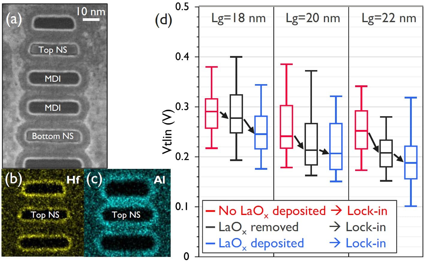
Figure 6 – (a-b-c) CFET-based test vehicle with integrated dipole-middle approach to form the gate stack (scanning TEM images and energy-dispersive x-ray spectroscopy (EDS) maps); (d) demonstration of the Vt reduction obtained after shifter lock-in (as presented at 2026 VLSI).
Wrapping up Part I: improving CFET-specific integration modules
With an improved module for backside contacting and a CFET-compatible approach to multi-Vt tuning, imec, together with its ecosystem of partners, demonstrates continued progress in integrating CFET-critical modules. These integration efforts are essential to ensure CFET’s introduction in the logic technology roadmap – most likely from A7 onwards.
In part 2, we will highlight through DTCO studies innovative standard cell architectures for sCFETs, ensuring CFET’s scalability across multiple logic nodes.
This work has been enabled in part by the NanoIC pilot line. The acquisition and operation are jointly funded by the Chips Joint Undertaking, through the European Union’s Digital Europe (101183266) and Horizon Europe programs (101183277), as well as by the participating states Belgium (Flanders), France, Germany, Finland, Ireland and Romania. For more information, visit nanoic-project.eu.
This article was originally published in Semiconductor Engineering.
Want to know more?
[1] ‘Towards a process flow for monolithic CFET transistor architectures,’ imec reading room, 2023;
[2] ‘Performance boosters to scale monolithic CFET across multiple logic technology nodes,’ S. Yang et al., imec Reading Room, 2025;
[3] ‘Imec demonstrates functional monolithic CFET devices with stacked bottom and top contacts,’ imec Press Release, 2024;
[4] ‘Improved backside contacting for CFET,’ C. Sheng et al., 2026 VLSI;
[5] ‘Dipole-first gate stack as a scalable and thermal budget flexible multi-Vt solution for nanosheet/CFET devices,’ H. Arimura et al., 2021 IEEE International Electron Devices Meeting (IEDM), San Francisco, CA, USA, 2021, pp. 13.5.1-13.5.4, doi: 10.1109/IEDM19574.2021.9720527;
[6] ‘Dipole material-independent carrier mobility in dipole-first nMOS gate stack and introduction of multi-Vt patterning-tolerant dipole-middle integration for NS/CFET,’ H. Arimura et al., 2026 VLSI.