Imec is an international player, with global presence, employing more than 6,600 people. Through its R&D programs, imec gathers more than 600 industry partners, leading tech companies from across the worldwide semiconductor and deep-tech value chain, to jointly drive innovation in microchips and its applications such as AI, health, automotive, space and security, compute and connectivity, industry & consumer. In 2025, imec continued to reinforce its leadership position, building on its legacy of top-notch R&D, global partnerships and innovation.
Our shortlist of highlights:
Imec driving innovation in Flanders and Europe
Imec holds a strategic position in the global semiconductor ecosystem, setting the pace in Flanders as well as in Europe’s Chips Act ambitions, to boost the region’s economy.
With 203 patent applications, representing an 8.6 percent increase over the previous year, imec was Belgium's top patent applicant for the second year in a row, according to the European Patent Office (EPO) Patent Index 2024, published in March 2025. Moreover, Belgium ranked fourth in Europe for the number of patent applications submitted by public research organizations (PRO), with imec accounting for 7 out of 10 Belgian PRO patent applications between 2001 and 2020. These data reflect imec's leadership role in innovation within Europe.
In 2025, the grant of the NanoIC pilot line project was signed between imec and the Chips JU, marking the official start of this prestigious and ambitious project. The first tenders for the acquisition of equipment were released, with many more to come, and the first state-of-the-art tools are currently being installed, complementing imec’s pilot line with unique advanced capabilities and capacity, needed to speed up R&D learning cycles, better support industry partners, and boost innovation across the globe.
In the framework of the NanoIC pilot line, ASML and imec signed strategic partnership agreement in March 2025 to install ASML’s whole product portfolio, including its High NA EUV scanner (EXE:5200), the most advanced tool available, in imec’s cleanroom. Preparations for the installation of the EXE:5200 are ongoing. Imec also intensified its collaboration with ZEISS, with the extension of their strategic partnership and additional investments of ZEISS in imec's pilot line. In total, almost 100 semiconductor tools will be installed in imec’s pilot line as part of the NanoIC project. This large capacity and capability extension will reinforce imec’s status as the most advanced R&D pilot line in the world.
In October 2025, the NanoIC pilot line released a major update of imec’s N2 pathfinding PDK, adding advanced SRAM memory macros and other features. Such advanced PDKs empower researchers and designers to learn and innovate with full SoC architectures, explore next generation semiconductor technologies, address complex design challenges; supporting innovation in beyond 2nm nodes.

Management ASML and imec
Imec welcomed Henna Virkkunen, Executive Vice-President of the European Commission for Technological Sovereignty, Security and Democracy, to its headquarters in Leuven, to discuss the implementation of the European Chips Act, ideas for its revision in 2026, and how imec contributes to ensuring long-term economic resilience and competitiveness through cutting-edge R&D and global collaboration.

Henna Virkunnen visiting imec.
In March 2025, the aCCCess Project was launched, a four-year, EU-funded project to connect the Competence Centers, Pilot Lines, and Design Platform. The project aims to accelerate innovation and provide businesses with easier access to technology and funding.
In April 2025, imec was selected as the coordinator of a consortium of 12 European partners to develop the EU Chips Design Platform. Funded by Chips Joint Undertaking, the platform will improve access to semiconductor design infrastructure, training, and capital for fabless startups, SMEs, and research organizations.

Representatives of the twelve consortium members gathered at the International Iberian Nanotechnology Laboratory in Braga, Portugal.
In September 2025, a consortium of European partners, with imec as one of the key partners, launched the STARLight project, to drive advances in Silicon Photonics on 300mm wafers and push the boundaries of optical interconnect solutions for Datacenters & AI, Telecommunications, Automotive & LiDAR.
In October, imec was selected as the coordinator of the BE-AI Factory Antenna under the EuroHPC Joint Undertaking (EuroHPC JU). This BE-AI Factory Antenna will provide Belgian companies, researchers and public institutions with expert services for developing and deploying large-scale AI models, access to AI-optimized supercomputing infrastructure, access to high-quality, interoperable datasets, and training on using the infrastructure and the datasets.
Leveraging and strengthening its global leading position in semiconductor R&D, imec is expanding its global presence in strategically important regions. Imec’s internationalization strategy is built on creating mutual opportunities: by expanding globally, imec gains access to diverse talent pools and regional expertise, while offering local partners and ecosystems the chance to collaborate on world-leading innovation. This approach fosters knowledge exchange and accelerates technological breakthroughs. Imec connects new hubs and fabs worldwide, thereby maximizing local impact. Each initiative complements its Flemish foundation, ensuring coherence, excellence, and shared growth across all activities.
In Malaga (Spain), with the support of the Governments of Andalucia and Spain, preparations are ongoing to build a new cleanroom and offices. The new facility will focus on R&D and low-volume manufacturing of specialty components and processes for new applications in domains such as health, automotive, and infotainment and will work closely together with the 300mm fab in Leuven. Karel van Gils was appointed as regional managing director, and the first local employees were hired.
In October, a new office in Heilbronn (Germany) was inaugurated. This Advanced Chip Design Accelerator competence center is supported by the Governments of Baden-Württemberg and Germany to support the automotive industry with state-of-the-art chiplet technology, strengthening Baden-Württemberg’s innovation ecosystem while fueling international impact.
Imec also deepened its commitment to driving innovation in the Netherlands as a strategic partner in the ChipNL Competence Center that was launched in October 2025. In May, Jesse Robbers was appointed as regional managing director of imec The Netherlands. Also in May, the Holst Centre Photonics Lab was opened together with TNO. This lab is partly funded by PhotonDelta to accelerate innovation in integrated photonics and stimulate collaboration between industry and academia.

Visit of imec Spain site.
Global impact
Imec strongly advocates that the success of the chip industry lies in unity and global collaboration. The EU, Asia and the USA should reinforce and complement each other, providing a critical mass to accelerate innovation. Underscoring this vision, imec is extending its strategic partnerships with technology centers with complimentary expertise and infrastructure.
In May, imec announced a partnership with MIT (Boston) to explore how advanced semiconductor technologies can enable personalized treatment and diagnostic devices to improve quality of life. In October, imec officially opened a new imec USA office in San Jose, (California) in the presence of Minister-President of Flanders Matthias Diependaele, further strengthening imec’s footprint at the heart of the world’s innovation ecosystem.

Opening of the imec San Jose office.
At the economic mission of Flanders Investment & Trade to Tokyo and Osaka in June, imec deepened ties in Japan. In the presence of Minister-President Diependaele, the strategic partnership with Tokyo Electron was extended, aimed at developing semiconductor nodes beyond 2nm. The decade-long partnership with Socionext on imec’s Core Partner Program was deepened in 2025, a confirmation of how imec brings application-focused value related to design, development and manufacturing for fabless and system companies. Imec also signed a Memorandum of Understanding (MOU) with Hitachi and RIKEN to accelerate the development of silicon quantum computers.

Imec and TEL during the signing ceremony of the extension of their partnership.
At Semicon Korea in February, imec and the National NanoFab Center (NNFC), South Korea’s top public semiconductor technology service provider, signed a Memorandum of Cooperation to collaborate on a joint internship program.
In November, imec announced its plans to set up a research hub in Doha (Qatar) that will focus on accelerating innovation, bringing IC-Link by imec’s chip design expertise to the Middle East, performing novel compute architecture research, and setting up development programs to strengthen the region’s semiconductor talent.
Leadership transition and reorganization
In September, imec announced a pivotal leadership transition that reinforces its long-term strategic vision and trusted global partnerships. After 17 years, Luc Van den hove will assume the role of Chairman of imec’s Board of Directors, effective April 2026, in providing strategic guidance and focus on executive stakeholder management, ensuring continuity and confidence across imec’s international partner ecosystem. Patrick Vandenameele was appointed by the Board of Directors as the next Chief Executive Officer of imec. Patrick will assume full leadership responsibilities in April 2026.

Luc Van den hove and Patrick Vandenameele.
Workforce development
Attracting diverse talents and developing talent through education is pivotal to support the further growth of the semiconductor industry. Imec’s workforce development activities aim at reaching out and educating global talent and assisting the global semiconductor ecosystem in this endeavor with a dedicated offering.
In May and October, imec organized student excellence days for European master and PhD students in STEM. These full-day events provided an introduction to the NanoIC pilot line, imec, the semiconductor industry and its career opportunities. In June and September, imec organized trainings on the N2 Pathfinding Process Design Kit (PDK), developed within the NanoIC pilot line. In September, imec launched a 2-day low barrier training on chips fabrication and the semiconductor industry, aimed to support industry and academia in their workforce development efforts.
From the imec tenure of Christian Haffner, breakthrough results demonstrating electro-optic performance record in thin-film strontium titanate at cryogenic temperatures were published in Science in October 2025. The achievement reflects how imec’s tenure track model backs bold, long-horizon research by offering high potential top researchers a team, protected time, access to advanced fabrication, and cross-disciplinary support to achieve top-notch scientific breakthroughs.
Sustainability
Imec’s sustainability efforts are closely aligned with the UN Sustainable Development Goals (SDGs), which guide its long-term ESG strategy and societal impact. Imec’s efforts were rewarded with the official recognition of imec as UN SDG Champion by Voka.
The imec.netzero tool is considered a standard imec’s partners in its Imec’s Sustainable Semiconductor Technologies and Systems (SSTS) program, to quantify and benchmark carbon, water, and material footprints for current and future CMOS technologies. Key results were reported on PFAS-free materials evaluation, semiconductor waste characterization, and the development of metrology and abatement solutions for hazardous waste.
R&D highlights
Compute technologies & systems
At the onset of the AI era, data processing needs show no signs of saturation. To meet this growing demand for real-time, energy-efficient compute solutions for AI-powered applications, from smart devices to datacenters and beyond, imec’s compute technologies and systems sector focuses on developing next-generation architectures and technologies that enable efficient, scalable, and secure data processing and data transfer across edge devices, high-performance computing, and advanced communication networks.
Compute system scaling
Dimensional scaling is becoming increasingly difficult, requiring technology solutions of staggering complexity. Imec’s technology-oriented programs, organized around logic, enabled by advanced patterning, 3D, memory (both active memory and storage), and optical IO, are the backbone of its core program. Within these programs, imec develops industry-relevant process steps, modules and (baseline) integration flows, and explores new materials and novel devices.
2025 highlights include the demonstration at ECTC 2025 of a 300mm RF silicon interposer platform combining exceptional performance and flexibility. The platform enables seamless integration of RF-to-sub-THz CMOS and III/V chiplets on a single carrier, achieving a record-low insertion loss of just 0.73dB/mm at frequencies up to 325GHz. The achievement paves the way for compact, low-loss, and scalable next-generation RF and mixed-signal systems.

Imec’s 300mm RF silicon interposer platform for chiplet-based heterogeneous integration.
At IITC2025, imec demonstrated Ru lines at 16nm pitch with resistance as low as 656Ω/µm, using a semi-damascene integration flow optimized for cost-effective manufacturability, making it an attractive approach for fabricating the first local interconnect metal layer of the A7 and beyond technology nodes. With 20 imec contributions at IITC2025, imec confirmed its leading role in advancing the interconnect roadmap for the next ten years.
At IEDM 2025, imec presented advances in 2D-material based device technology beyond state of the art in collaboration with leading semiconductor manufacturers. Collaboration with TSMC resulted in record performing WSe2 -based pFETs (with Imax as high as 690µA/µm), using a fab-compatible process flow. A partnership with Intel led to improved fab-compatible modules for source/drain contact formation and gate stack integration (with reduced equivalent oxide thickness (EOT)).
Imec’s team of world-class experts in advanced patterning is recognized for its prolific output of scientific papers and research breakthroughs. Their expertise spans the full spectrum of lithography and patterning challenges, from scanner and mask co-optimization to advanced etch and metrology. At SPIE Advanced Lithography + Patterning, imec presented the first electrical test (e-test) results obtained on 20nm pitch metal line structures patterned after single-exposure High NA EUV lithography. The e-test results confirmed the capability of the High NA EUV lithography scanner and its surrounding ecosystem to pattern lines/spaces at such a small dimension. In September, at the 2025 SPIE Photomask Technology + EUV Lithography Conference, imec confirmed its leadership with new milestones in single patterning High NA EUV lithography for both damascene and direct metal etch metallization processes. Highlights included demonstrations of advanced line-space patterning and direct metal etch of ruthenium, with yields and uniformities relevant for future interconnect scaling. Also in September, imec started preparing its cleanroom for the installation of the ASML EXE:5200 High NA EUV scanner, which is foreseen for Q2 2026.

Installation of the EXE:5200 High NA EUV scanner pedestal in imec’s cleanroom.
Beyond traditional technology scaling – XTCO, quantum computing and superconducting computing
Not only are computing needs continuing to grow, they are also becoming increasingly application-specific. As the AI and computing landscape evolves, advancements in technology alone will not be sufficient to meet future requirements for performance and power efficiency. For all actors in the semiconductor industry to optimally address these challenges, we need continuous dialogue between applications and technology. Imec is therefore looking into alternative technology and system-level solutions that go beyond classical computing, such as CMOS2.0, superconducting and quantum computing.
In 2025, imec enriched its program offering with a cross-technology co-optimization program (XTCO). This new XTCO program is structured around five pillars addressing the system scaling challenges in the realm of their application constraints: compute density, power delivery, thermal performance, memory density & bandwidth, and compute fabric (network architectures). By connecting deep-technology building blocks to the system, imec’s new program structure aims to better serve every player within the semiconductor ecosystem.
At IEDM2025, imec presented its first XTCO results: a combination of cross-layer optimization with broad technological expertise resulted, under realistic AI training workloads, in a reduction of peak temperatures from 140.7°C to 70.8°C in a 3D HBM-on-GPU (high-bandwidth memory on graphical processing unit), a promising compute architecture for next-gen AI applications, on par with current 2.5D integration options.
At Super Computing 2025, imec announced the launch of imec.kelis, a cutting-edge analytical performance modeling tool designed to revolutionize the design and optimization of AI datacenters. Imec.kelis provides an end-to-end framework for evaluating system performance across compute, communication, and memory subsystems. It is tailored for large language model (LLM) training and inference workloads, offering fast, accurate, and generalizable predictions validated on industry-standard platforms. Early adopters are already experimenting with the tool, signaling strong market interest.
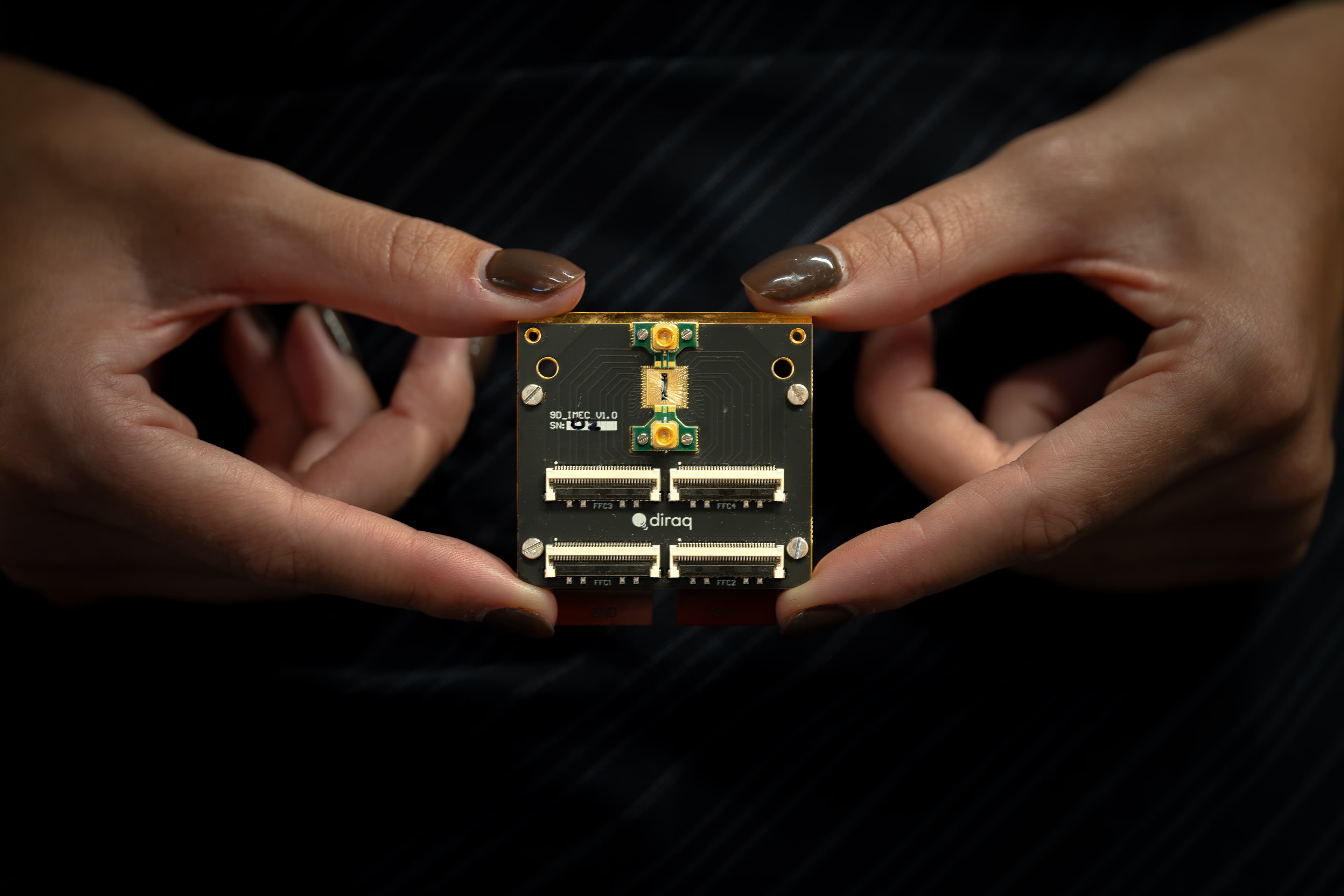
Since almost a decade, imec is optimizing and engineering spin-qubit fabrication, leveraging advanced 300mm CMOS processes, to support the transition of quantum technologies from laboratory prototypes to scalable, industrial-grade platforms. In September 2025, imec and Diraq published a paper in Nature, demonstrating silicon qubits, made using industrial processes, that consistently show error rates surpassing quantum error correction needs. For the first time, silicon MOS-based quantum-dot spin-qubit devices realized with industrial manufacturing techniques performed as well as academic reference devices.
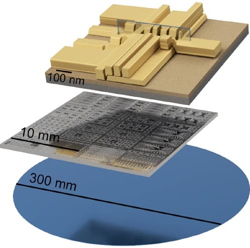
Schematic of a Diraq two-qubit device on a 300mm wafer, showing the full wafer, single die and single device level.
In June 2025, BeQCI, a consortium funded by the EU and the Belgian Science Policy Office and with imec as strategic partner, deployed the first cross-border Measurement Device Independent QKD (MDI QKD) link between Belgium and Luxembourg. This is a major milestone in the 30-month quantum cryptography project, which aims to achieve a way to transmit data 100% safe and uninterceptably, using quantum physics principles.
Superconducting digital logic is considered as a promising path for large-scale, high-performance, and energy-efficient computing. Imec’s superconducting compute strategy aims at developing scalable, CMOS-compatible superconducting digital technologies that can deliver up to 100x higher energy efficiency and 10–100x better performance than current CMOS processors. At IEDM2025, imec presented advancements in its NbTiN-based superconducting technology platform, including Higher JJ densities thanks to a novel Josephson junction process module, improved circuit reliability through functional flux-trapping mitigation structures and enhanced superconducting properties of NbTiN, expanding the operational window. At the PTW, the new program offering on superconducting computing was introduced to imec’s partners, and partnership negotiations are ongoing.
Connected Computing
To deliver real-time, energy-efficient compute solutions for AI powered applications, imec also looks into the next-generation of wired and wireless communication technologies and systems that enable seamless, high-speed, reliable and secure data communication.
In January, imec published in Nature a significant milestone in silicon photonics with the successful demonstration of electrically-driven GaAs-based multi-quantum-well nano-ridge laser diodes fully, monolithically fabricated on 300mm silicon wafers in its CMOS pilot prototyping line. This breakthrough provides a pathway to the development of cost-effective and high-performance optical devices for applications in data communications, machine learning and artificial intelligence.
In June, imec and its research groups at the Ghent University (Photonics Research Group and IDlab) published in Nature Communications a fully-integrated, single-chip microwave photonics system for compact and versatile high-frequency signal processing. This chip can replace bulky and power-hungry components, enabling faster wireless networks, low-cost microwave sensing, and scalable deployment in applications like 5G/6G, satellite communications, and radar systems.
Also, at VLSI 2025, imec and IDLab announced a 7-bit 150 GSa/s Digital-to-Analog Converter (DAC), fabricated in a 5nm FinFET CMOS process that achieves data rates of up to 300 Gb/s using PAM-4 modulation. The high-speed DAC paves the way for faster and more energy-efficient optical and electrical links in data centers.

Imec’s new DAC combines high speed and energy efficiency.
In October at ECOC 2025, imec debuted a beyond-110GHz C-band GeSi electro-absorption modulator on its 300mm silicon photonics platform. Achieving a net data rate of 400Gb/s per lane, imec’s GeSi EAM heralds a new generation of compact, high-bandwidth, low-latency, and energy-efficient modulators – tailored for short-reach, scale-up optical interconnects, and manufacturable at silicon scale.
Industry & Consumer
Imec is developing a wide range of semiconductor and digital technologies including sensor and actuator, energy, or communication technology, and software solutions, to deliver scalable innovation across domains such as industrial automation, consumer electronics, sustainable energy infrastructure, ... , focusing on a select number of platforms where its mastery of advanced nanotechnology offers unique value.
At IEDM 2025, imec successfully demonstrated the cointegration of metasurfaces with colloidal quantum dot photodiodes (QDPDs) on its 300 mm CMOS pilot line. This pioneering approach enables a scalable platform for the development of compact, miniaturized high-resolution shortwave infrared (SWIR) sensors, paving the way for broad application in security, agriculture, automotive, aerospace, and beyond.
At VLSI 2025, imec showed record-breaking RF GaN-on-Si transistor performance for high-efficiency 6G power amplifiers. It demonstrated both a gallium nitride (GaN) MOSHEMT (metal-oxide-semiconductor high-electron-mobility transistor) on silicon with record efficiency and output power, and a contact module with record-low resistance of 0.024Ω·mm. These advancements are crucial for next-gen 6G and set new standards for efficiency and output power for enhancement-mode (E-mode) mobile applications at low supply voltage.
Also in 2025, imec launched a 300mm GaN program track focusing on GaN epi growth and HEMT process flows for low and high voltage power electronics. AIXTRON SE, GlobalFoundries, KLA, Synopsys Inc and Veeco are the first partners, underlining full ecosystem development. The use of 300mm wafers enables the development of more advanced, efficient and cost-effective devices, including low-voltage point-of-load converters for CPUs and GPUs.
Within the EnergyVille framework, imec works alongside partners KU Leuven, Vito and UHasselt to advance sustainable energy technologies and smart energy systems. Imec’s R&D in this field include PV technology and systems, smart grid solutions, and battery and power-to-molecules technology. In January 2025, imec and the University of Cyprus demonstrated long-term outdoor stability of imec’s 4x4cm perovskite solar modules. While current perovskite solar modules show a retention efficiency lasting weeks, imec’s modules achieved, in real-world conditions, a remarkable power efficiency retention of 78 percent after one year. These promising findings are among the first results to address the stability issues that currently hinder perovskite solar cells from commercialization.

Solar perovskite mini-module.
Automotive
Imec’s automotive sector includes technology and sensor fusion developments for Advanced Driver Assistance Systems (ADAS) and in-cabin sensing, and imec’s automotive chiplet program (ACP) that brings together automotive and semiconductor stakeholders in a pre-competitive research initiative aimed at accelerating chiplet and packaging technologies in next-gen vehicles, meeting automotive-grade requirements for safety and reliability. Additionally, imec is working on technologies and solutions for wireless communication between vehicles and their environments.
In March 2025, imec pioneered a photonic code-division multiplexing FMCW 144GHz distributed radar system that ensures coherent chirps to remote radar units. Demonstrating successful range measurements, imec’s proof-of-concept paves the way for multi-node radar systems with superior angular resolution compared to single-node setups. A world-first that could revolutionize next-generation driver assistance solutions and other high-precision sensing applications.

Close up of imec's proof-of-concept photonics-enabled code-division multiplexing (CDM) frequency-modulated continuous wave (FMCW) 144GHz distributed radar system.
In October 2025, imec announced that GlobalFoundries (GF) joined imec’s Automotive Chiplet Program (ACP) as a foundry partner. GF will provide advanced manufacturing capabilities to support the development and manufacturing of the ACP’s automotive-ready, chiplet-based platforms. Semiconductor and system companies Infineon, Silicon Box, STATS ChipPAC, and Japanese autonomous driving technology developer TIER IV also committed to join ACP, expanding imec’s automotive ecosystem. Imec’s Advanced Chip Design Accelerator (ACDA) in Heilbronn (Germany) was officially opened in October. It will support the automotive industry with state-of-the-art chiplet technology, strengthening Baden-Württemberg’s innovation ecosystem while fueling international impact. Moreover, a strategic alignment initiative between imec’s Automotive Chiplet Program (ACP) and Japan’s ASRA consortium was initiated to standardize automotive chiplet architectures.
Health
Semiconductor technologies are revolutionizing healthcare, driving advances from research to diagnosis and therapy. Imec is leveraging its technology expertise to develop next-generation solutions that improve drug discovery and development, support early diagnosis, and achieve more effective treatments.
In May 2025, Merck Group and imec established a strategic partnership to develop a disruptive highly adaptable modular system that integrates cutting edge organoid biology models with fit-for-purpose biosensing and microfluidic capabilities. The system aims to redefine drug discovery and development by producing more reliable predictions and real-time identification of human organ responses to drug and chemical stimuli with application in pre-clinical safety, toxicity studies and DMPK (Drug Metabolism and Pharmacokinetics).
At ITF World, imec demonstrated a highly miniaturized ingestible sensor, live on stage. The sensor prototype, developed at OnePlanet Research Center, is three times smaller than current capsule endoscopies and the first to provide redox balance measurements. It can provide valuable insights into intestinal inflammation, the gut microbiome, and overall health.

Picture of the ingestible sensor.
In a Nature Communications paper imec and the Feinstein Institutes for Medical Research demonstrated that intermittent interferential current stimulation (i²CS) allows for more targeted peripheral nerve activation, reducing off-target side effects and enhancing stimulation efficacy. It unlocks novel therapy possibilities for chronic diseases.
In Nature Neuroscience, imec and its partners introduced the Neuropixels 1.0 NHP neural probe, a high-density electrode array enabling brain-wide single neuron recordings in nonhuman primates. With up to 4,416 electrodes and recordings from 3,000+ neurons in a single session, this breakthrough provides researchers with unprecedented access to deep and superficial brain structures, opening new doors for studying brain function and disorders.
At IEDM2025, imec demonstrated first wafer-scale fabrication of solid-state nanopores using EUV lithography. Nanopore technology is considered a gamechanger for genomics and proteomics, offering a high-throughput platform of biosensor arrays for biosensing and sequencing. By demonstrating wafer-scale fabrication, imec transforms the technology from a lab-scale concept into a scalable platform that could accelerate personalized.
Imec venturing
Imec uses its nanoelectronics, digital technology expertise, and venturing experience to launch spin-offs, and help tech and digital startups enter the market successfully.
The imec spin-off Vertical Compute was launched in January 2025, raising €20 million to revolutionize the future of AI computing by tackling AI’s compute memory bottleneck with a novel vertical integrated memory and compute technology. Eyeo, another imec spin-off, started in May 2025, raising €15 million. Eyeo's breakthrough color-splitting photonics innovation drastically improves light sensitivity and breaks sensor resolution limits, ushering in a new era in ultra-compact, high-performance imaging.

3D rendering of eyeo’s waveguide structure
Also in 2025, imec signed a strategic development agreement with Openchip to drive the development of cutting-edge artificial intelligence (AI) systems that seamlessly integrate hardware and software, pushing the boundaries of AI innovation. A collaboration was signed with Hypervision Surgical to co-develop scalable on-chip hyperspectral imaging (HSI) solutions for surgical applications. In December, Marvell announced the acquisition of Celestial AI, a U.S.-based venture backed by imec.xpand. Celestial AI is a strong example of how imec’s deep-tech venturing strategy, combining access to imec’s disruptive semiconductor technologies, unique infrastructure and ecosystem, and funding helps deep-tech startups scale globally.
IC-link by imec
In May, imec significantly expanded the IC-Link by imec offering, taking mature, best-in-class technologies from imec’s R&D pipeline and making them commercially available. Through IC-Link by imec, imec's 200mm photonics platform is now available for prototyping and manufacturing of advanced photonics integrated circuits.