Logic CMOS scaling
Imec pushes Moore’s law to the extreme by scaling down the dimensions of logic devices and exploring new paths on the system level.
Worldwide, technology innovations are being developed to allow CMOS scaling to go on for at least another decade. Many of these breakthroughs originate or are developed towards manufacturability at imec.
However, dimensional scaling of logic devices does no longer provide the performance-per-unit benefit as it did in the past. To realize further gains, we now also need DTCO (design technology co-optimization) and STCO (system-technology co-optimization).
2025 press release: Curvilinear technology: a game changer for the logic technology roadmap
These evolutions will be enabled by new architectures, materials and integration schemes, and advances in EUV and high-NA EUV patterning. All these advances will be studied, tested and further developed in lockstep. Imec, as an industry-wide hub for expertise, equipment and materials is the ideal place for this co-development.

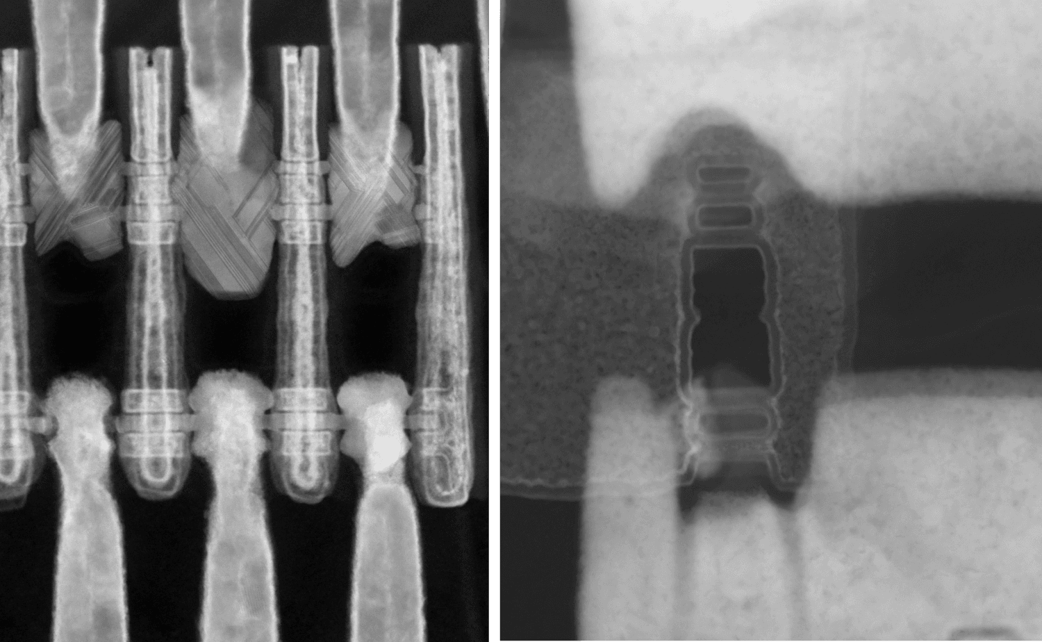
CMOS scaling beyond FinFET towards sub-1nm
Today, FinFET devices are the mainstream transistor architectures, with the most advanced nodes having 2 fins in a 6-track (6T) standard cell. The next generation of transistors, vertically stacked nanosheet devices, will enable scaling the track height of standard cells down to five tracks (5T). Further scaling may then be facilitated by forksheets – a unique imec innovation.
The follow-up is the generation of 4-track cells. A promising candidate for this is the CFET (complementary FET), where n- and p-devices are stacked into a compact footprint.
Our scientists are already looking further, towards the 1nm technology nodes and beyond. We’re working to introduce 2D materials and atomic channels. With these exciting developments, sub-4-track cells come into consideration.
EUV lithography innovations for CMOS scaling
This drive to smaller dimensions will be pushed by further developments in EUV patterning. Imec, together with its strategic partner ASML, continuously advances EUV lithography, for example by investigating stochastic defectivity – which could lead to improved throughput and cost.
Still, multiple EUV exposures will be needed to enable pitch scaling, which will increase the cost and complexity of the process. Eventually, we expect high-numerical-aperture (high-NA) EUV lithography to become available for patterning of the most critical layers of the industry’s 1nm node. This technique will push the multi-patterning of some of these layers back to single patterning, providing cost, yield and cycle-time relief.
In the high-NA lab, ASML and imec perform research on the manufacturing of the most advanced nanoscale devices with high-NA EUV and assist the ecosystem of equipment and material suppliers to prepare for the introduction of high-NA EUV technology to the industry.
Read this article for more info on the next generation of patterning technology
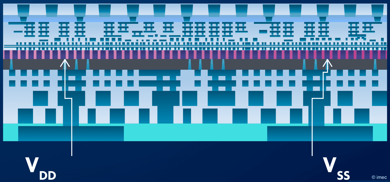
System-technology co-optimization (STCO)
In addition to dimensional scaling, new materials innovations in both front-end and back-end are needed to boost the performance. Beyond that and to obtain even larger performance gains, STCO will come into play. STCO will allow identifying technology solutions to address system issues like the memory wall, power distribution or SoC sub-system partitioning. Imec’s goal is to identify and mature the technology knobs that are needed by STCO to improve the system-level performance.
Beyond CMOS
Imec is also exploring beyond-CMOS solutions, breaking away from the fundamentals of classical computation. With these paradigm-changing technologies, we do not aim to replace CMOS circuits, but rather complement them in a hybrid, multi-device architecture. In these architectures, the new technologies will be used to do what they’re good at, e.g. high-performance computing, or ultralow-power operation.
One example of a beyond-CMOS paradigm is quantum computing. Another is majority gate computing, where the result or output of a computation is determined by a majority sampling of multiple inputs. With this principle, gates can be built for arithmetic circuits that promise to be much more compact and energy-efficient than the conventional NAND-based circuits. The imec team is investigating and benchmarking three different implementations of majority gates: spin-wave majority gates, spin torque majority gates and plasmonic majority gates.
Want to join our research into logic CMOS scaling?